Zener Diode MCQ Question And Answer
1. Zener diode is designed to specifically work in which region without getting damaged?
a) Active region
b) Breakdown region
c) Forward bias
d) Reverse bias
Answer - b
The Zener diode is a specifically designed diode to operate in the breakdown region without getting damaged. Because of this characteristic, it can be used as a constant-voltage device.
2. What is the level of doping in Zener Diode?
a) Lightly Doped
b) Heavily Doped
c) Moderately Doped
d) No doping
Answer - b
A Zener diode is heavily doped so that the breakdown voltage occurs at a lower voltage. If it were lightly/moderately doped, it would breakdown at a comparatively high voltage and, thus, would not be able to serve its purpose.
3. When the reverse voltage across the Zener diode is increased _____________
a) The value of saturation current increases
b) No effect
c) The value of cut-off potential increases
d) The value of cut-off potential decreases
Answer - c
As the frequency of the incident radiation increases, the kinetic energies of the emitted electron are higher and therefore require more repulsive force to be applied to stop them.
The value of saturation current increases, as the intensity of the incident radiation, increases.
The value of cut-off potential decreases, as the frequency decreases.
4. Zener Diode is mostly used as ____________
a) Half-wave rectifier
b) Full-wave rectifierc
c) Voltage Regulator
d) LED
Answer - c
The Zener diode, once in the breakdown region, keeps the voltage in the circuit to which it is connected as constant. Thus it is widely used as a voltage regulator.
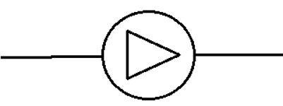
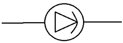
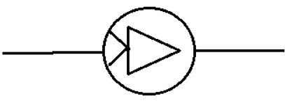
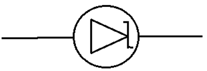
5. Which of the following is the correct symbol for the zener diode?
The Zener diode, once in the breakdown region, keeps the voltage in the circuit to which it is connected as constant. Thus it is widely used as a voltage regulator.
5. Which of the following is the correct symbol for the zener diode?
6. In normal junctions, the breakdown is same as Zener breakdown.
a) True
b) False
Answer - b
a) True
b) False
Answer - b
In normal p-n unction diodes, the breakdown takes place by avalanche breakdown which is different than the Zener breakdown. Zener diode is specifically made to operate in that region.
7. The depletion region of the Zener diode is ____________
a) Thick
b) Normal
c) Very Thin
d) Very thick
View Answer
Answer: c
Zener diode is fabricated by heavily doping both p- and n-sides of the junction, which results in an extremely thin depletion region.
8. The electric field required for the field ionization is of what order?
a) 104 V/m
b) 105 V/m
c) 106 V/m
d) 107 V/m
Answer: c
In a Zener diode, a very high electric field is produced for even a very small voltage. The electric field required for field ionization is of the order 106 V/m.
9. In a circuit the load current is 5 mA and the unregulated output is 10 V. If the voltage drop across the Zener diode is 3 V, what should be the value of resistance?
a) 50 Ωb
b)100 Ωc
c)125 Ωd
d)150 ΩA
Answer: d
The value of R should be such that the current through the Zener diode is much larger than the load current.
Imagine Iz = 20 mA. The total current is therefore 24 mA.
Thev voltagedrop = 3 V
Resistance = 3 V/24 X 10-3 AR=125 Ω.
Viva Questions
1) What is a zener diode?
A heavily doped P-N junction which has a sharp breakdown voltage is called as a zener diode.
2) What is diode?
The diode is a semiconductor device having p-n junction.
3) On what factor does the breakdown voltage of a zener diode depends?
The breakdown voltage of a zener diode depends upon the amount of doping. If the diode is heavily doped, the depletion layer will be thin and consequently the breakdown of the junction will occur at a lower reverse voltage.
4) What is breakdown voltage?
When the reverse bias of a zener diode is increased, a critical voltage is reached at which the reverse current increases sharply to a high value. This critical voltage is called breakdown voltage.
5) What is the difference between an ordinary diode and a zener diode?
i) A zener diode is like an ordinary diode except that it is properly doped so as to have a sharp break down voltage.
ii) It has a sharp breakdown voltage called zener voltage.
iii) When forward biased, zener diode characteristics are just that of ordinary diode.
iv) A zener diode is always reverse biased.
6) Why zener diode is always reverse biased?
Because it utilize reverse characteristics for acting like a voltage regulator.
7) Mention the uses of zener diode.
A zener diode is used as a voltage regulator to provide a constant voltage from a source whose voltage vary over sufficient range.
8) What do you mean by Characteristics of a Zener Diode?
A Graph showing the variation of voltage applied across the terminals of a diode to the corresponding current is called characteristics of a diode. In case of junction diodes, there are two types of characteristics, forward and reverse characteristics.
9) Explain the flow of current in zener diode under reverse biasing condition?
In case of reverse biasing condition, the external field is established in a direction such as to help internal field. Under this biasing the holes in P- region and electrons in N- region are pushed away from the junction with the result that the depletion or barrier layer is thickened and hence increases the potential barrier, therefore, the flow of current stops. Only a few thermally generated minority carriers produce a very small current.
10) Explain the flow of current in zener diode under forward biasing condition?
In the case of forward biasing condition, the zener diode behaves like an ordinary p-n junction diode. In this case the external field is established in a direction such as to oppose the internal field. The external field is much stronger than internal field. In this arrangement holes move along the external field from p-region to n-region and electrons move opposite to the field from n-region to p-region, that is, the majority carriers from each side move across the junction. The potential barrier or depletion layer at the junction wiped out and a substantial current flows depending upon the density of n- and p- carriers.
11) What do you mean by doping?
The process of introducing the impurity in a semiconductor is called doping.
12) What is Zener breakdown?
If the reverse potential across the zener diode is increased beyond a certain value, the current increases very rapidly due to zener breakdown. Zener breakdown occurs when the applied electric field or potential is so high that the valence band electrons are pulled out to the conduction band in large numbers resulting in breakdown. Thus, a zener breakdown, direct rupture of covalent bonds take place by thermally generated carriers having acquired high energy due to strong electric field.
13) What do you mean by avalanche breakdown?
When the reverse voltage is made sufficiently high the thermally generated electrons and holes acquire high energy from the applied potential and make ionizing collisions with the atoms of the crystal. These collisions produce further electrons, which in turn collide with further atoms. The commutative effect of such collisions results in the breakdown of the junction. Due to this avalanche multiplication the reverse current increases abruptly to high value. This is called avalanche breakdown and may damage the junction.
14) What are the differences between avalanche breakdown and zener breakdown?
In general zener breakdown occurs below 8V and avalanche breakdown occurs at higher voltages (~20 V). The Zener breakdown is characterized by the soft knee, whereas avalanche breakdown is hard knee type. Zener breakdown voltage has a negative temperature coefficient, while the avalanche breakdown voltage exhibits positive temperature coefficient.
15) How the width of the depletion region in the reverse biased diode varies with the impurity concentration.
The width of the depletion region of a reverse biased diode varies as the square root of the impurity concentration.
16). How the value of the potential barrier depends on the amount of doping of the semiconductor?
The value of potential barrier decreases with heavy amount of doping of the semiconductor.
17). Why the silicon diode is preferred compare to germanium diode?
Silicon diodes are preferred compare to germanium diodes because of its higher temperature to current capability.
18). Under what condition a zener diode behaves like an ordinary p-n junction diode?
A zener diode behaves as an ordinary p-n junction diode when it is used in forward bias conditions.
19). What is the main application of a zener diode?
An important application of zener diode is its use as voltage regulator. The regulating action takes place due to the fact that in reverse breakdown region; a very small change in voltage produces a very large change in current.


