Julius Edgar Lilienfeld(April 18, 1882 – August 28, 1963) was an Austro-Hungarian American physicist and electical engineer, credited with the first patents on the field-effect transistor (FET) (1925) and electrolytic capacitor (1931). Because of his failure to publish articles in learned journals and because high-purity semiconductor materials were not available yet, his FET patent never achieved fame, causing confusion for later inventors.
Lilienfeld moved to the United States in 1921 to pursue his patent claims, resigning his professorship at Leipzig to stay permanently in 1926. In 1928, he began working at Amrad in Malden, Massachusetts, later called Ergon Research Laboratories owned by Magnavox, which closed in 1935. In the United States Lilienfeld did research on anodic aluminum oxide films, patenting the electrolytic capacitor in 1931, the method continuing to be used throughout the century. He also invented an "FET-like" transistor, filing several patents describing the construction and operation of transistors, as well as many features of modern transistors.
The optical radiation emitted when electrons strike a metal surface is named "Lilienfeld radiation" after he first discovered it close to X-ray tubeanodes. Its origin is attributed to the excitation of plasmons in the metal surface.
The American Physical Society has named one of its major prizes after Lilienfeld.
The field-effect transistor (FET) is an electronic device which uses an electric field to control the flow of current. FETs are devices with three terminals: source, gate, and drain. FETs control the flow of current by the application of a voltage to the gate, which in turn alters the conductivity between the drain and source.
Types of FET Transistor
FETs are of two types- JFETs or MOSFETs. JunctionFET
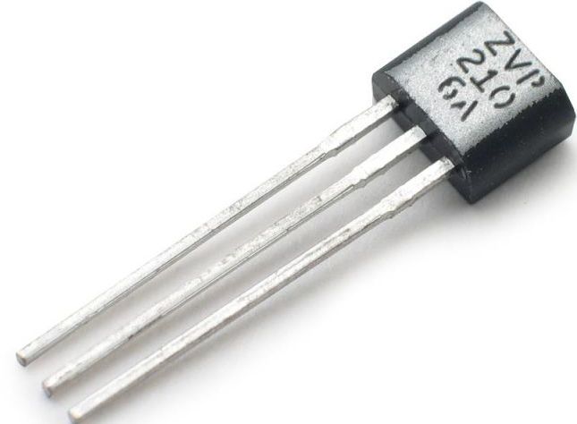
A Junction FET
The Junction FET transistor is a type of field effect transistor that can be used as an electrically controlled switch. The electric energy flows through an active channel between sources to drain terminals. By applying a reverse bias voltage to gate terminal, the channel is strained so the electric current is switched off completely.
The junction FET transistor is available in two polarities which are;
N- Channel JFET
N channel JF
N channel JFET consists of an n type bar at the sides of which two p type layers are doped. The channel of electrons constitutes the N channel for the device. Two ohmic contacts are made at both ends of the N-channel device, which are connected together to form the gate terminal. The source and drain terminals are taken from the other two sides of the bar. The potential difference between source and drain terminals is termed as Vdd and potential difference between source and gate terminal is termed as Vgs. The charge flow is due to flow of electrons from source to drain. Whenever a positive voltage is applied across drain and source terminals, electrons flows from the source ‘S’ to drain ‘D’ terminal , where as conventional drain current Id flows through the drain to source. As current flows through the device, it is in on state. When a negative polarity voltage is applied to the gate terminal, a depletion region is created in the channel. The channel width is reduced, hence increasing the channel resistance between the source and drain. Since the gate source junction is reverse biased and no current flows in the device, it is in off condition. So basically if voltage applied at the gate terminal is increased, less amount of current will flow from the source to drain. The N channel JFET has greater conductivity than the P channel JFET. So the N channel JFET is more efficient conductor compared to P channel JFET.
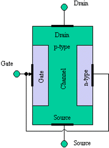
P-Channel JFET
P channel JFET consists of a P type bar, at two sides of which n type layers are doped. The gate terminal is formed by joining the ohmic contacts at both the sides. Like in an N channel JFET, the source and drain terminals are taken from the other two sides of the bar. A P type channel, consisting of holes as charge carriers, is formed between source and drain terminal.
P channel JFET bar
A negative voltage applied to the drain and source terminals ensure the flow of current from source to drain terminal and the device operates in ohmic region. A positive voltage applied to the gate terminal ensures the reduction of channel width, thus increasing the channel resistance. More positive is the gate voltage; less is the current flowing through the device.
Circuit Diagram
Characteristics of p channel Junction FET Transistor
Given below is characteristic curve of p channel Junction Field Effect transistor and different modes of operation of the transistor.
Characteristics of p channel junction FET transistor
Cutoff region: When the voltage applied to the gate terminal is enough positive for the channel width to be minimum, no current flows. This causes the device to be in cut off region.
Ohmic region: The current flowing through the device is linearly proportional to the applied voltage until a breakdown voltage is reached. In this region, the transistor shows some resistance to the flow of current.
Saturation region: When the drain source voltage reaches a value such that the current flowing through the device is constant with the drain source voltage and varies only with the gate source voltage, the device is said to be in saturation region.
Break down region: When the drain source voltage reaches a value which causes the depletion region to break down, causing an abrupt increase in the drain current, the device is said to be in breakdown region. This breakdown region is reached earlier for lower value of drain source voltage when gate source voltage is more positive.
MOSFET Transistor
MOSFET transistor
MOSFET transistor as its name suggests is a p type (n type) semiconductor bar (with two heavily doped n type regions diffused into it) with a metal oxide layer deposited on its surface and holes taken out of the layer to form source and drain terminals. A metal layer is deposited on the oxide layer to form the gate terminal. One of the basic applications of field effect transistor is using a MOSFET as a switch.
This type of FET transistor has three terminals, which are source, drain, and gate. The voltage applied to the gate terminal controls the flow of current from source to drain. The presence of an insulating layer of metal oxide results in the device having high input impedance.


 P channel JFET consists of a P type bar, at two sides of which n type layers are doped. The gate terminal is formed by joining the ohmic contacts at both the sides. Like in an N channel JFET, the source and drain terminals are taken from the other two sides of the bar. A P type channel, consisting of holes as charge carriers, is formed between source and drain terminal.